|
|
Home | Audio | DIY | Guitar | iPods | Music | Brain/Problem Solving | Links| Site Map
This work is licensed under a Creative Commons License.
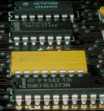 |
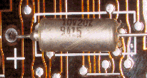
Discrete
components are the backbone of the electronics world, consisting of
individually packaged, leaded devices, highly integrated circuits (IC),
interconnects, terminators, switches, etc. While discretes are rapidly being displaced by the smaller-form surface mount technology (SMT) package, the discrete component is still widely in use, especially in extreme environmental applications where the SMT device will not perform reliability and/or is unavailable. |
 |
 |
GENERAL REQUIREMENTS
|
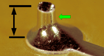
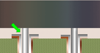
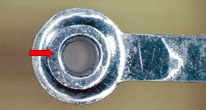
PREFERRED100% SOLDER FILL (PTH)
|
 |
 |
PREFERREDPWB COMPONENT SIDE FILLET (PTH)
|
PREFERREDSOLDER SIDE FILLETS (PTH/NPTH)
|
 |
 |
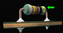
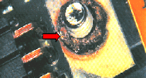
PREFERREDHEAT PRODUCING PARTS |
PREFERREDHIGH-MASS COMPONENTS |
 |
 |
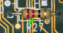
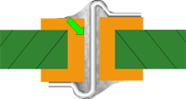
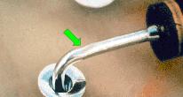
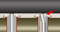
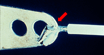
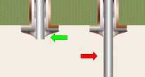
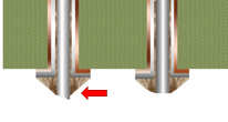
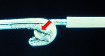
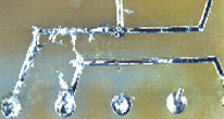
PREFERREDWIRE/LEAD INSULATION GAP
|
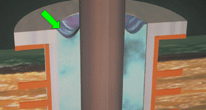
PREFERREDWIRE/LEAD INSULATION GAP
|
 |
 |
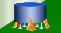
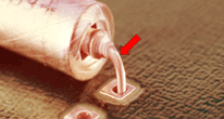
ACCEPTABLEADHESIVES |
UNACCEPTABLEADHESIVE INCLUSION
|
 |
 |
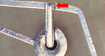
ACCEPTABLECLINCHED LEAD TERMINATION
|
UNACCEPTABLEIMPROPERLY CLINCHED LEAD
|
 |
 |
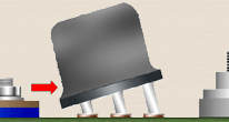
ACCEPTABLECONDUCTIVE CASE PARTS
|
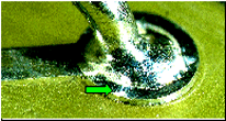
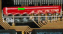
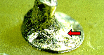
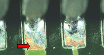
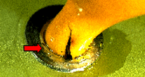
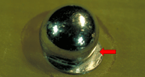
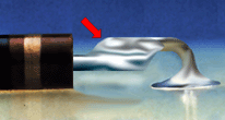
ACCEPTABLEDEWETTING
|
 |
 |
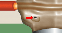
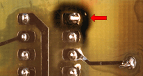
ACCEPTABLEEXPOSED BASE METAL
|
UNACCEPTABLEEXPOSED BASE METAL
|
 |
 |
ACCEPTABLEEXPOSED BASE METAL
|
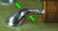
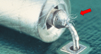
ACCEPTABLEFILLER WIRE USE
|
 |
 |
ACCEPTABLEGLASS ENCASED PARTS
|
UNACCEPTABLEUNSLEEVED GLASS ENCASED PARTS
|
 |
 |
ACCEPTABLELEAD PROTRUSION LENGTH
|
UNACCEPTABLEINSUFFIENCT LEAD PROTRUSION
|
 |
 |
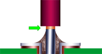
ACCEPTABLEINTERFACIAL CONNECTIONS/VIAS
|
ACCEPTABLESOLDER-FILLED INTERFACIAL
|
 |
 |
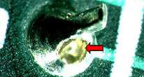
ACCEPTABLEMEASLING
|
UNACCEPTABLEMEASLING
|
 |
 |
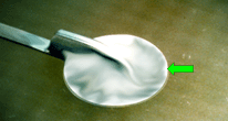
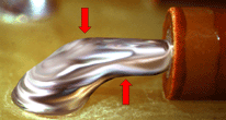
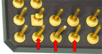
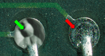
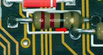
ACCEPTABLENON-UNIFORM/UNEVEN FLOW |
UNACCEPTABLE UNEVEN FLOW/REFLOW |
 |
 |
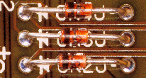
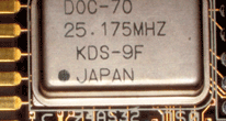
ACCEPTABLEPART MARKINGS
|
UNACCEPTABLEIDENTIFICATION MARKS MISSING
|
 |
 |
ACCEPTABLEPITS |
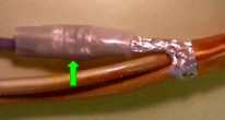
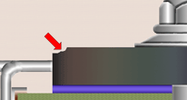
ACCEPTABLESHRINK TUBING
|
 |
 |
ACCEPTABLESMOOTH TOOL IMPRESSION MARKS
|
ACCEPTABLESOLDER FILLET RECESS/SHRINKBACK
|
 |
 |
ACCEPTABLESOLDER IN STRESS RELIEF BEND
|
UNACCEPTABLESOLDER IN STRESS RELIEF BEND
|
 |
 |
ACCEPTABLETEMPERED LEADS
|
UNACCEPTABLEBENT TEMPERED LEADS
|
 |
 |
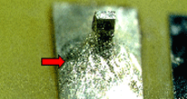
UNACCEPTABLEBLOWHOLE
|
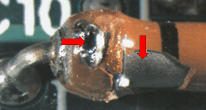
UNACCEPTABLEBRIDGING
|
 |
 |
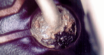
UNACCEPTABLECHARRING
|
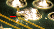
UNACCEPTABLECHIP-OUTS (NICKS)
|
 |
 |
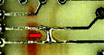
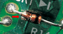
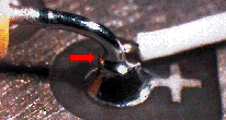
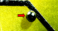
UNACCEPTABLECOLD SOLDER JOINT
|
UNACCEPTABLECONTAMINATION
|
 |
 |
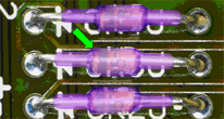
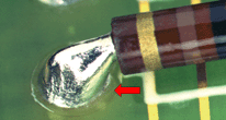
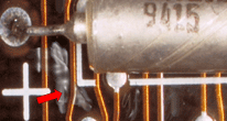
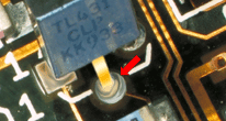
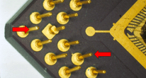
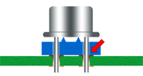
UNACCEPTABLECOPLANARITY
|
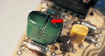
UNACCEPTABLECRACKS (COMPONENT)
|
 |
 |
UNACCEPTABLECRACKS (LAMINATE)
|
UNACCEPTABLECRACKS (SOLDER FILLET)
|
 |
 |
UNACCEPTABLEDAMAGED PART SEAL
|
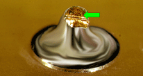
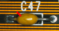
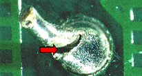
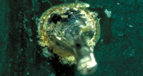
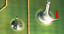
UNACCEPTABLEDEWETTING
|
 |
 |
UNACCEPTABLEDISCOLORED LAMINATE (BURNS)
|
UNACCEPTABLEDISCOLORED LAMINATE
|
 |
 |
UNACCEPTABLEDISTURBED SOLDER
|
UNACCEPTABLEEXCESS SOLDER
|
 |
 |
UNACCEPTABLEEXCESS SOLDER/SOLDER FLOODING
|
UNACCEPTABLEEXCESSIVE LEAD PROTRUSION
|
 |
 |
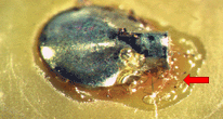
UNACCEPTABLEEXPOSED DIE/CIRCUIT ELEMENTS
|
UNACCEPTABLEEYELETS
|
 |
 |
UNACCEPTABLEFLUX RESIDUE
|
UNACCEPTABLEFLUX SPLATTER
|
 |
 |
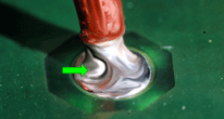
UNACCEPTABLEFRACTURED SOLDER
|
UNACCEPTABLEGOLD INTERMETALLIC
|
 |
 |
UNACCEPTABLEGOLD PLATING
|
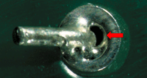
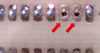
UNACCEPTABLEHOLE OBSTRUCTION
|
 |
 |
UNACCEPTABLEIMPROPER LEAD BENDING
|
UNACCEPTABLEIMPROPER LEAD CUTTING
|
 |
 |
UNACCEPTABLEIMPROPER LEAD LENGTH
|
UNACCEPTABLEIMPROPER ORIENTATION
|
 |
 |
UNACCEPTABLEIMPROPER TINNING
|
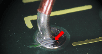
UNACCEPTABLEINSUFFICIENT SOLDER
|
 |
 |
UNACCEPTABLEINSUFFICIENT STRESS RELIEF/LEAD BEND
|
UNACCEPTABLEMENISCUS CONTACT
|
 |
 |
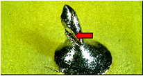
UNACCEPTABLENICKS
|
UNACCEPTABLENONWETTING
|
 |
 |
UNACCEPTABLENO FLOW/REFLOW
|
UNACCEPTABLENO SOLDER
|
 |
 |
UNACCEPTABLEOBSCURED SOLDER TERMINATIONS
|
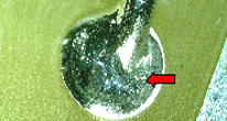
UNACCEPTABLEOPENS/VOIDS
|
 |
 |
UNACCEPTABLEOVERHEATED SOLDER
|
UNACCEPTABLEPART BODY CONTACT
|
 |
 |
UNACCEPTABLEPART LEADS USED AS TERMINALS
|
UNACCEPTABLEPART MISALIGNMENT
|
 |
 |
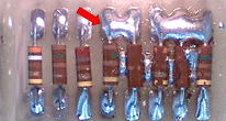
UNACCEPTABLEPIGGYBACKED PARTS
|
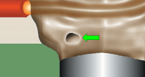
UNACCEPTABLEPINHOLE
|
 |
 |
UNACCEPTABLEPOOR WETTING
|
UNACCEPTABLEPOPCORNING
|
 |
 |
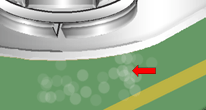
UNACCEPTABLEPOROUS SOLDER
|
UNACCEPTABLEROSIN SOLDER JOINT
|
 |
 |
UNACCEPTABLESCRATCHES (SOLDER FILLET)
|
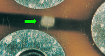
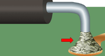
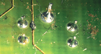
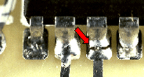
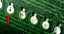
UNACCEPTABLESOLDER BALLS
|
 |
 |
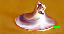
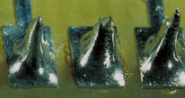
UNACCEPTABLESOLDER PEAKS, ICICLES, SHARP EDGES
|
UNACCEPTABLESOLDER SKIPS
|
 |
 |
UNACCEPTABLESOLDER SLIVERS
|
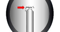
UNACCEPTABLESOLDER SPLATTER
|
 |
 |
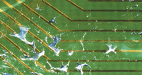
UNACCEPTABLESOLDER WEBBING |
UNACCEPTABLESPLICED CONDUCTORS/LEADS
|
 |
 |
UNACCEPTABLEVOIDS
|
UNACCEPTABLEWHISKER
|
Home | Audio | DIY | Guitar | iPods | Music | Links | Site Map | Contact
![]()